Home | SiteMap | Contact Us | Korean
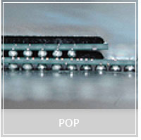
POP(Package on Package)

 
Product Overview

Cell phones, pocket PCs and other consumer products require the maximum functional integration of memory, DSPs, ASICs, RFs, MEMs and other devices in the smallest footprint and lowest profile. As a result, die stack package which consists of more than two dies interconnected by wire bond in one package has been developed and manufactured. But it has some issues such as compound yield loss, test complexity and KGD issue related to IC cost. POP basically consists of pre-tested good packages interconnected using solder balls or wires and has advantages over die stack package such as high final test yield and flexibility of procuring top and bottom packages independently from multiple sources.

Features
 

- Die Stack Package has been developed for 3D Package.
- But it has some issues such as compound yield loss, test complexity and KGD issue
  related to IC cost
- PoP is the more remarkable than others because of its superiority of Test yield &
  complexity & KGP.

 
Key Features
 Wafer thickness (mm)  Min. 0.075
 Substrate  2 / 4 (BT)
 Solder ball pitch (mm)  Min. 0.5


© 2015 ASE Korea, Inc. All Rights Reserved. Terms of Use